In the ever-evolving world of technology, there is a silent hero that plays a crucial role in powering our modern devices—the silicon wafer. These tiny, circular slices of silicon serve as the foundation for electronic components, enabling the creation of advanced microchips, processors, and integrated circuits. Behind these remarkable wafers lies the expertise and innovation of Silicon Wafer Manufacturers, who tirelessly work to push the boundaries of technology. We will explore the fascinating world of silicon wafer manufacturing, uncovering the intricate processes involved, and highlighting the industry's impact on technological advancements.
Understanding Silicon Wafers:
- Definition and Composition
Before delving into the manufacturing process, let us understand what silicon wafers are and what makes them so essential in the realm of electronics. A silicon wafer, often referred to as a semiconductor wafer, is a thin, disc-shaped substrate made of silicon. Silicon is a widely abundant chemical element, making it an ideal material for mass production.
Silicon wafers are usually manufactured using single-crystal silicon or polycrystalline silicon. Single-crystal wafers are highly valued due to their superior electrical properties. Polycrystalline wafers, on the other hand, are more cost-effective but exhibit slightly lower performance. These wafers come in various sizes, typically ranging from 100 millimeters to 300 millimeters in diameter, with the larger sizes becoming increasingly prevalent in recent years.
- Importance in Electronics
Silicon wafers form the fundamental building blocks of electronic devices. They act as a platform upon which electronic components and circuits are constructed, enabling the integration of transistors, diodes, and other electronic elements. The manufacturing process involves precise doping and etching techniques to modify the properties of the silicon, allowing the creation of intricate electronic structures on a microscopic scale.
Without silicon wafers, the vast array of devices we rely on daily, such as smartphones, computers, and even automobiles, would cease to exist in their current form. The relentless pursuit of smaller, faster, and more energy-efficient devices relies heavily on advancements in silicon wafer manufacturing.
Silicon Wafer Manufacturing Process:
- Crystal Growth
The first step in silicon wafer manufacturing is crystal growth. This process involves creating a single-crystal ingot of silicon, which will later be sliced into wafers. The most common method used for crystal growth is the Czochralski process.
In the Czochralski process, high-purity silicon is melted in a quartz crucible at temperatures exceeding 1,400 degrees Celsius. A seed crystal, typically made of single-crystal silicon, is immersed into the molten silicon and slowly withdrawn while rotating. As the seed crystal is pulled, it solidifies, allowing the formation of a large cylindrical crystal, known as an ingot.
- Ingot Slicing
Once the silicon ingot has been grown, it undergoes a meticulous slicing process to transform it into individual wafers. The ingot is first polished to achieve a flat, mirror-like surface. Then, using a diamond saw, the ingot is sliced into thin wafers. This process requires precision and control to ensure consistent thickness and minimize waste.
- Wafer Grinding and Polishing
After slicing, the wafers undergo a grinding and polishing process to refine their thickness and achieve a mirror-like finish. Grinding machines equipped with abrasives remove any excess material and reduce the wafer thickness to the desired dimensions. Subsequently, the wafers go through a chemical-mechanical planarization (CMP) process, which employs a combination of chemicals and polishing agents to remove surface irregularities and achieve an ultra-smooth surface.
- Doping and Photolithography
Doping is a critical step in the manufacturing process that imparts specific electrical properties to the silicon wafers. Doping involves introducing controlled amounts of impurities, such as boron or phosphorus, into the silicon lattice. This process modifies the conductivity of the silicon, allowing it to function as either a positive or negative semiconductor.
Once the wafers have been doped, photolithography techniques come into play. A photosensitive material, called a photoresist, is applied to the wafer's surface. Then, a photomask, containing a pattern of the desired circuitry, is placed over the wafer. Ultraviolet light is directed onto the mask, exposing the photoresist in specific areas. The exposed or unexposed regions are later chemically treated, resulting in the creation of intricate circuit patterns.
- Etching and Deposition
Etching and deposition processes are employed to further refine the circuit patterns on the silicon wafers. Etching selectively removes specific areas of the silicon, shaping the circuit elements with high precision. There are various etching techniques available, including wet etching and dry etching (plasma etching), each with its advantages and applications.
Deposition, on the other hand, involves the application of thin layers of materials onto the wafer's surface. Chemical vapor deposition (CVD) and physical vapor deposition (PVD) are commonly used methods for depositing materials like silicon dioxide or metal films onto the wafer. These layers serve as insulators, conductors, or other functional components, depending on the specific requirements of the circuit design.
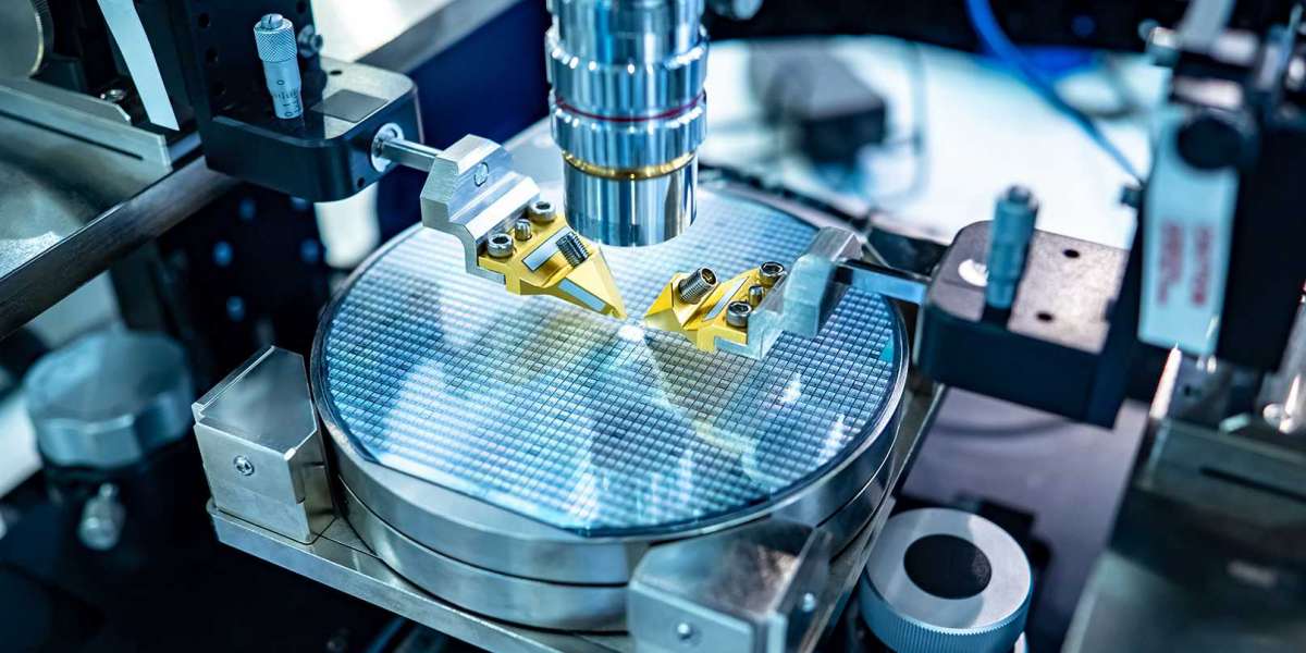
- Testing and Quality Control
As the manufacturing process nears completion, stringent testing and quality control measures are implemented to ensure the wafers meet the required specifications. Electrical tests assess the performance of individual wafers, checking for defects, impurities, and uniformity. Optical inspection systems scan the wafer surfaces, detecting any abnormalities or imperfections that could impact device functionality.
Technological Advancements and Future Prospects:
The relentless pursuit of technological advancements drives continuous innovation in silicon wafer manufacturing. The demand for smaller, more powerful electronic devices necessitates the development of wafers with higher performance, improved energy efficiency, and increased yield. Here are some key areas of advancement and future prospects for silicon wafer manufacturers:
- Wafer Size
Over the years, there has been a steady increase in wafer size, with 300-millimeter (12-inch) wafers becoming the industry standard for advanced semiconductor manufacturing. Larger wafers offer several advantages, including higher productivity and lower production costs per chip. However, the transition to larger wafer sizes presents numerous technical challenges, requiring advancements in equipment, materials, and manufacturing processes.
- Finer Circuitry
The constant drive for smaller and more powerful devices has led to the development of advanced fabrication techniques, such as extreme ultraviolet lithography (EUVL) and multi-patterning. These methods enable the creation of finer circuitry and higher transistor densities on the wafers. Silicon wafer manufacturers must continuously innovate to push the limits of miniaturization while maintaining high yields and reliability.
- Novel Materials
The exploration of new materials beyond traditional silicon has gained significant attention in recent years. Silicon carbide (SiC) and gallium nitride (GaN) are examples of wide-bandgap materials that offer superior electrical properties, enabling high-performance devices with reduced power consumption. Silicon wafer manufacturers are exploring ways to integrate these novel materials into their manufacturing processes, opening doors to a new era of semiconductor technology.
- Advanced Packaging
As the complexity of electronic systems increases, advanced packaging techniques have become essential to meet the industry's demands. Three-dimensional integrated circuits (3D-ICs) and system-on-chip (SoC) technologies require innovative packaging solutions, such as through-silicon vias (TSVs) and micropumps. Silicon wafer manufacturers are actively collaborating with packaging companies to develop integrated solutions that optimize performance, size, and power consumption.
- Emerging Technologies
Silicon wafer manufacturing is not limited to traditional semiconductor applications. It plays a vital role in emerging technologies, such as the Internet of Things (IoT), artificial intelligence (AI), and quantum computing. These fields require specialized silicon wafers designed to meet unique performance criteria. Silicon Wafer Manufacturers are at the forefront of these developments, working closely with technology companies to enable the next wave of innovation.
Conclusion:
Silicon wafer manufacturers are the unsung heroes behind the technological advancements that shape our modern world. Through intricate processes and relentless innovation, these manufacturers pave the path for smaller, faster, and more powerful electronic devices. From crystal growth to circuit patterning, each step in the manufacturing process is carefully orchestrated to ensure the production of high-quality silicon wafers.