In the vast world of technology, where innovation is the driving force, one essential component stands tall as the foundation of countless electronic devices. the silicon wafer. Silicon wafers serve as the building blocks of integrated circuits (ICs) and are crucial for the production of semiconductors. As demand for advanced electronic devices continues to surge, the importance of Silicon Wafer Manufacturers cannot be overstated. We will explore the fascinating world of silicon wafer manufacturing, its processes, challenges, and the role it plays in empowering technological advancements.
The Genesis of Silicon Wafers:
Silicon wafers have a rich history that can be traced back to the mid-20th century when scientists and engineers began experimenting with silicon as a potential material for semiconductors. Silicon, with its unique properties of being a semiconductor and its abundance in the Earth's crust, quickly became the material of choice for electronic components. This led to the birth of silicon wafer manufacturing as a critical industry.
The Manufacturing Process:
- Silicon Ingot Growth
The first step in silicon wafer production is the growth of silicon ingots. The process begins with high-purity silicon, typically sourced from quartzite or quartz. The silicon is then heated to extremely high temperatures and combined with a seed crystal of single-crystal silicon. As the molten silicon cools, a solid crystal structure is formed around the seed crystal, resulting in a cylindrical silicon ingot.
- Ingot Slicing
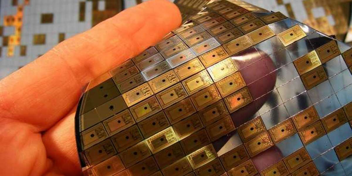
Once the silicon ingot has been grown, it is sliced into thin circular discs known as wafers. This slicing process involves using a diamond saw or a wire saw to cut the ingot into individual wafers. The thickness of the wafers may vary depending on the intended application, with common thicknesses ranging from 200 to 800 micrometers.
- Wafer Surface Preparation
After slicing, the wafers undergo a rigorous surface preparation process to ensure their purity and smoothness. This process typically involves several steps, including cleaning, etching, and polishing. Cleaning removes any impurities or contaminants from the wafer surface, while etching removes the damaged layer caused by slicing. Finally, polishing creates an ultra-smooth surface, ready for subsequent processing.
- Doping and Deposition
Doping is a crucial step in semiconductor manufacturing, as it introduces specific impurities into the silicon wafers to modify their electrical properties. This process involves depositing precise amounts of dopant materials onto the wafer surface. Deposition techniques such as chemical vapor deposition (CVD) or physical vapor deposition (PVD) are commonly employed to ensure uniform dopant distribution across the wafer.
- Photolithography and Etching
Photolithography is a key process in semiconductor manufacturing that involves creating intricate patterns on the wafer surface. A photosensitive material called a photoresist is applied to the wafer, followed by exposure to ultraviolet light through a photomask. This exposes specific areas of the wafer, allowing for selective etching or deposition of materials. The etching step removes the unwanted materials, leaving behind the desired pattern.
- Thermal Processing
Thermal processing steps, such as oxidation and annealing, are employed to further enhance the electrical properties of the silicon wafers. Oxidation involves exposing the wafer to high temperatures in the presence of oxygen, forming a thin layer of silicon dioxide on the surface. Annealing, on the other hand, is a heat treatment process that helps relieve stress and repair crystal defects, improving the overall quality of the wafers.
- Testing and Packaging
Once the silicon wafers have undergone all the necessary fabrication steps, they are subjected to rigorous testing to ensure their functionality and quality. Various electrical tests are conducted to assess the performance of the integrated circuits embedded within the wafers. After testing, the wafers are packaged, usually in trays or cassette holders, to protect them from damage during transportation.
Challenges in Silicon Wafer Manufacturing:
The production of silicon wafers is a complex and highly demanding process, often facing several challenges along the way. Some of the major challenges include:
- Cost-Effectiveness
As the demand for advanced electronic devices continues to rise, silicon wafer manufacturers face the constant challenge of producing wafers at a competitive cost. The production process involves several expensive steps, including high-purity material sourcing, specialized equipment, and cleanroom facilities. Manufacturers must continually optimize their processes and explore new technologies to achieve cost-effectiveness without compromising quality.
- Yield Enhancement
Achieving high yield rates is crucial in silicon wafer manufacturing to minimize waste and maximize productivity. The complex nature of the fabrication process, coupled with the delicate nature of Silicon Wafers, presents challenges in maintaining consistent yields. Any defects or impurities introduced during the manufacturing process can lead to yield loss. Manufacturers invest significant resources in research and development to improve yield rates and minimize production losses.
- Technological Advancements
The semiconductor industry is known for its rapid pace of technological advancements. As new technologies emerge, silicon wafer manufacturers must adapt to meet the evolving demands of the market. This includes keeping up with shrinking feature sizes, new material requirements, and novel fabrication techniques. Staying at the forefront of technological advancements requires continuous innovation, collaboration, and investment in research and development.
Empowering Technological Advancements:
Silicon wafer manufacturers play a pivotal role in empowering technological advancements across various sectors. The production of high-quality and reliable silicon wafers enables the development of advanced electronic devices that shape our modern world. From smartphones and laptops to medical devices and automotive electronics, silicon wafers serve as the backbone of innovation.
The continuous improvement in silicon wafer manufacturing processes allows for the production of smaller and more powerful integrated circuits. This drives the development of faster processors, higher-capacity memory chips, and more efficient sensors. These advancements fuel breakthroughs in artificial intelligence, the Internet of Things, renewable energy, and many other fields.
Moreover, silicon wafer manufacturers contribute to the growth of the global economy. The demand for silicon wafers creates employment opportunities and drives investments in research and development. The industry's constant pursuit of higher efficiency and performance not only benefits end-users but also drives down the cost of electronic devices, making technology more accessible to people around the world.
Conclusion:
Silicon wafer manufacturers are the unsung heroes behind the scenes, driving the technological advancements that shape our lives. Their relentless pursuit of excellence in fabrication processes, yield enhancement, and technological innovation is crucial to meet the demands of a fast-paced and ever-evolving industry. As we continue to embrace a future driven by technology, the role of silicon wafer manufacturers will remain pivotal in empowering the advancements that shape our world.